The main distinguishing element of modern nano optics over conventional optics is the strong confinement of plasmon fields at the surface of noble metal nanostructures. Noble metal surfaces and particles with sub-wavelength dimensions exhibit optical eigenmodes called surface plasmon polaritons which can be resonantly excited. Once excited, it is possible to strongly enhance the optical near-field and to resonantly enhance the scattering as well as absorption of light. The scientific exploration of plasmonic properties is appealing since it promises to overcome limitations imposed by classical optics, such as e.g. the Abbe limit of diffraction. Thus metal-dielectric surfaces and nanoparticles allow tailoring the flux of light in volumes significantly smaller than the wavelength and are therefore very attractive objects to study in nano optics.
To understand, monitor and finally control the plasmonic properties of nanosized objects, the information of the optical nearfield has to be collected by spectroscopic means with high spatial resolution. However, in the direction normal to the surface, the electric field strength drops off exponentially in most cases and is not transferred into the far-field. Nowadays this challenge is overcome by a variety of different (scanning) nearfield optical microscopy (SNOM) techniques. SNOM exploits the properties of evanescent waves by placing a tip very close to the specimen surface. This allows for the surface inspection with high spatial resolution. With this technique, the resolution of the image is limited by the size of the SNOM tip and not by the wavelength of the illuminating light. In particular, lateral resolution of 20 nm and vertical resolution of 1 nm have been demonstrated.
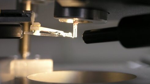
In our group, we develop and operate various nearfield microscopy setups to address different purposes, such as plasmonic waves propagating on noble metal surfaces, locally excited plasmon-polariton eigenmodes in metal-dielectric nanomaterials and metamaterials, or chemically synthesized nanostructures such as semiconductor nanowires. As one particular example, our group investigates the generation of a specific class of non-diffracting surface waves, so called plasmonic Airy beams, propagating on the surface of a gold film. Besides operating commercially available aperture and apertureless (scattering) SNOM setups, our group has put major efforts into the development of new SNOM techniques using two SNOM tips simultaneously on the same sample. Here, one tip is fed by an input signal exciting the probe at one local spot of the sample while the other tip collects the information on the field distribution from a different spot, disclosing the nearfield Green's function. Furthermore we operate heterodyne-based SNOM setups for simultaneous access to amplitude- and phase-resolved optical nearfields. With all these techniques, we aim to provide a versatile toolbox that allows for the precise characterization and manipulation of plasmon excitation schemes on arbitrarily complex and heterogeneously nanostructured surfaces.