Published:
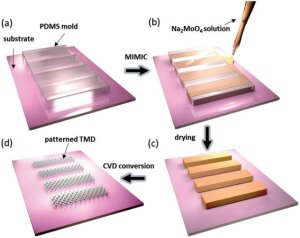
This process enables the patterned growth of TMDs
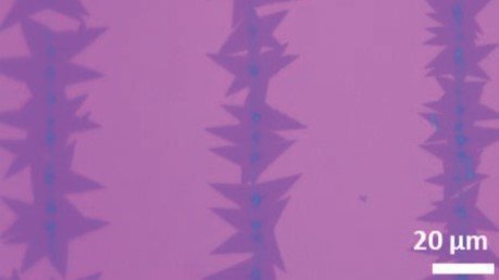
Image: Ziyan GanThe CVD-based growth of 2D-materials, such as TMDs, used to be spray&pray. Crystals would grow all over your sample, without any measure of control.
In a new publications in Small Methods entitled Patterned Growth of Transition Metal Dichalcogenide Monolayers and Multilayers for Electronic and Optoelectronic Device ApplicationsExternal link, we show controlled and localized growth of monolayer MoS2 and MoSe2 and optical & optoelectronic apps.
This work was headed by the team of Andrey Turchanin and Antony George at Friedrich-Schiller-Universität Jena with support by Sai Shradha, Fatemeh Abtahi and Tobias Vogl from the Institute of Applied physics as well as the Fraunhofer IOF, the Max Planck School of Photonics and the Leibniz-Institut für Photonische Technologien.
Great job, Ziyang Gan, Emad Najafidehaghani and Seung Heon Han for pushing through with this ambitious piece of research.
We acknowledge support by the Deutsche Forschungsgemeinschaft (DFG) - German Research Foundation via CRC 1375 NOA, the Bundesministerium für Bildung und Forschung as well as the Thüringer Aufbaubank.
