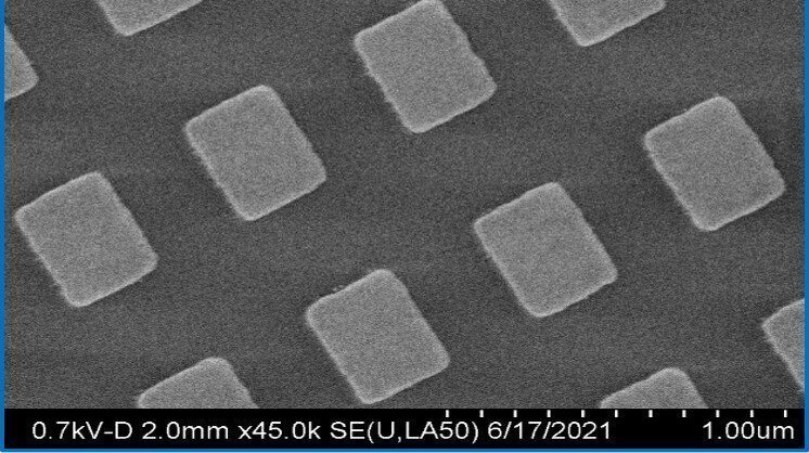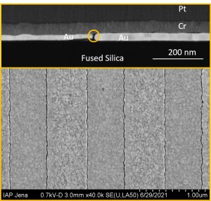
Gold nanogap-grating with <10nm gap dimensions for nonlinear plasmonics. Cross section (top) and top-view (bottom).
Picture: M.Steinert, IAP (University Jena)Plasmonic nanogap nanostructures consist of periodic metal-insulator-metal geometry where the nanogap is defined by the thickness of dielectric layer. The strong field enhancement arising from the extreme confinement of optical fields in the gap and combining it with optically resonant geometries could lead to a number of nonlinear optical effects. We are investigating nonlinear optical effects such as SHG, THG, HHG, and optically induced electron tunneling. This work is part of the Collaborative Research Center 1375 NOA (Nonlinear optics down to atomic scale, funded by the German Research Foundation (DFG)).
Our work focuses on the fabrication of plasmonic nanogap nanostructures using electron beam lithography, lift-off, planarization and employing atomic layer deposition to define the nanogaps well below 10 nm. With the established technology process, it is possible to realize complex shaped nanogap structures, which can find applications in sensing, frequency conversion, etc.
An additional research focus is on switchable components based on phase change materials such as VO2. Based on the realization of optical meta-structures in such materials we are investigating component designs which allow a full electrically controlled switching of optical functionalities for e.g. polarization control or beam steering.

